05. Electronics Production
From not knowing what a PCB is, to making one; this week has been about exploring a completely new territory. Hence, I’ll start from basics and expain everything electronics from basics, including the new terms I learned this week.
The goal of this week was to:
- Make an in-circuit programmer using milling.
- Optionally try doing the same using the plotter machine.
- Learn identifying and soldering the parts and components onto that PCB.
- Programme the PCB(FabISP).
- (Group)Characterize the specifications of your PCB production process.
What is a PCB?
A printed circuit board(PCB) mechanically supports and electrically connects electronic components or electrical components using
conductive tracks, pads and other features etched from one or more sheet layers of copper laminated onto and/or between sheet layers of a non-conductive substrate.
Components are generally soldered onto the PCB to both electrically connect and mechanically fasten them to it.
Printed circuit boards are used in all but the simplest electronic products.
Source : PCB - Wikipedia

An Example of a Printed Circuit Board(PCB) before and after attaching its componenents.
Identifying Electronic Components of a PCB
All electronic devices comprise of several different parts. These parts work together to modify and manage current and voltage to produce the desired effect. PCB’s act as backbones keeping everything connected and compacted in a form that is easy to use.
Circuit Boards : The circuit boards themselves are simple enough. They are just thin, plastic, rectangular plates with layer/layers of conductive copper foil on one or both sides. This copper is etched using milling or plotter machine after designing it as per one’s requirements.
If the copper traces behave like the skeleton of the PCB, acting as its basic structure – then the components are the vital organs. Each one has a different function. They give the circuit the unique qualities that make it fit for its intended purpose. Depending on the device or electronic item a PCB is designed for, different components will be needed for different circuits.
These components can consist of a wide range of electronic parts.
Battery : Provides the voltage to the circuit.

Resistors : Controls the electric current as it passes through them. They’re colour coded to determine their value.

LEDs : Light emitting diode. Lights up when current flows through it, and will only allow current to flow in one direction.

Transistor : Amplifies charge.

Capacitators : These are components which can harbour electrical charge.

Inductor : Stores charge and stops and change in current.

Diode : Allows current to pass in one direction only, blocking the other.

Switches : Can either allow current or block depending if they are closed or open.

Symbolic Chart

Diagrammatic Component Labels

Mounting components on a Printed Circuit Board(PCB)
These components can be mounted on a circuit board using one of the below methods:
-
Surface-mount technology : This is a method for producing electronic circuits in which the components are mounted or placed directly onto the surface of printed circuit boards (PCBs). An electronic device so made is called a surface-mount device (SMD).
An SMT component is usually smaller than its through-hole counterpart because it has either smaller leads or no leads at all. It may have short pins or leads of various styles, flat contacts, a matrix of solder balls (BGAs), or terminations on the body of the component. -
Through-hole technology : This refers to the mounting scheme used for electronic components that involves the use of leads on the components that are inserted into holes drilled in printed circuit boards (PCB) and soldered to pads on the opposite side either by manual assembly (hand placement) or by the use of automated insertion mount machines. Through-hole components are best used for high-reliability products that require stronger connections between layers. Whereas SMT components are secured only by solder on the surface of the board, through-hole component leads run through the board, allowing the components to withstand more environmental stress. This is why through-hole technology is commonly used in military and aerospace products that may experience extreme accelerations, collisions, or high temperatures.

Both technologies can be used on the same board for components not suited to surface mounting such as large transformers and heat-sinked power semiconductors.
Soldering
Soldering is one of the most fundamental skill needed to dabble in the world of electronics.
Solder, as a word, can be used in two different ways. Solder, the noun, refers to the alloy (a substance composed of two or more metals) that typically comes as a long, thin wire in spools or tubes. Solder, the verb, means to join together two pieces of metal in what is called a solder joint. So, we solder with solder!

Though, even after reading tutorials and watching videos, soldering is a skill that one needs to practice in order to master. No, arstist became one by watching others paint!
Group Work
After undertsanding this, we completed on the group assignment to get a better idea of the milling process. Complete documentation for that can be found here.
Since it was first time, everyone had to be a part of everything to understand the process.
Making a FabISP
What is a FabISP?
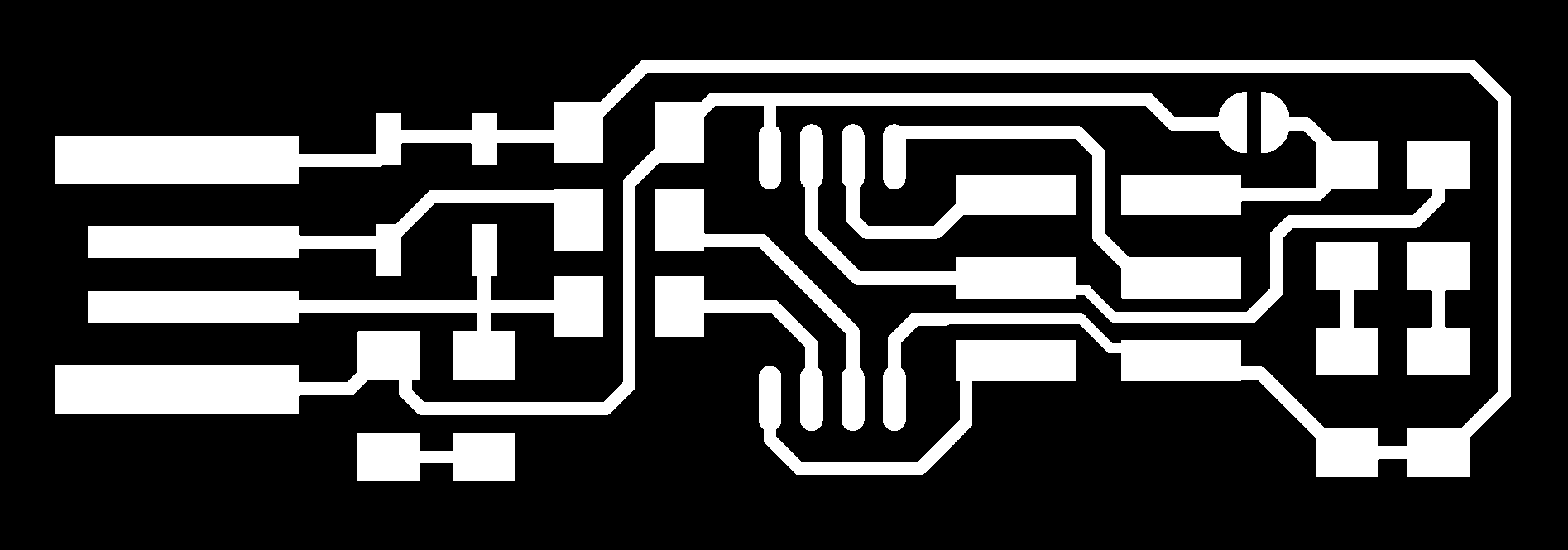
The FabISP is an in-system programmer for AVR microcontrollers, designed for production within a FabLab. That is, it allows you to program the microcontrollers on other boards you make, using nothing but a USB cable and 6-pin IDC to 6-pin IDC cable.
Over the years, there have been various versions of the FabISP and the one I’ve used is with ATtiny45.
Getting your PCB ready
This is the first step in making your circuit board. There are more than one ways to achieve this:
Using Milling Machine

This is the easier and more commonly used method for making your base circuit board. To start with you need seperate png files for you traces and outline of the board. The files for FabISP can be downloaded here:

- First thing we need to do is tape the back side of the copper board using a double sided tape in a way
so that no part of the surface is without tape and also, there is no overlapping of the tapes.
Once this is done, remove the other surface of the tape and stick it on the levelled surface of the sacrificial board of the milling machine.

Installing and setting up Fab Modules
The software used for milling is fabmodules which can be accessed from fabmodules.org
There is also a local version which can be downloaded and installed from here
(Note: For fabmodules to run, you need python which can be installed by entering sudo apt install python pip in terminal)
-
Once fab modules is running, go to terminal, and enter the following commands:
cd desktop
cd fabmodules
This will take you to the root directory where fab modules is installed. -
Next, enter npn start in terminal which is a command for connecting the server to the machine.

Once connected, go back to where we’ll be setting up the milling parameters.
- In Input Format, select image(.png) and from the pop-up window select the png file for traces of your PCB.

- In Output format, select Roland Mill(.rml).

- Select PCB Traces(1:64)

- Next is selcting the machine. It was MDX-20 in our case.
Once this is done, our file is set with the default output parameters.
Setting up the machine
- Next is inserting a 1/64 drill bit into the machine. This is a very delicate tool and can break easily hence it must be used very carefully.
- Once the bit is tightened in the machine, bring it down the z-axis using the up and down buttons on the machine. After it is close to the board, you can set the x and y using fabmodules and place it over the point which you want as your origin.
- Once x and y are set, loosen the bit and place it in a manner that its tip is resting on the copper board. This step needs to be done very carefully as these bits are delicate and expensive!

Using Fab modules
Note: Confirm the size of the PCB before proceeding further because with png format, it tends to change the scale when certain changes are made. (It blew up to almost 10 times the size it should be when I tried to rotate it by 90 degrees)

- The output parameters I used are:
Cut Depth : 0.1mm
Tool Diameter : 0.4
Number of offsets : 4
Offset overlapping : 50%
Once this is set, click on calculate and the computer should display the complete toolpath of the milling process.
Click on save to save the project and send to start the milling.

- The milling process should take a few minutes depending on the size of your pcb. The total time and the elapsed time is displayed on the computer screen.


- Next is cutting the PCB. For that select the cut file from image(.png) option. Output format is the same (.rml). And the bit is PCB Cutting 1/32.

-
For cutting, we need to increase the cut depth. I used the depth of 1.0mm.
-
Change the bit to 1/16 or 1/32(we only had 1/16) and all other process remains the same. The important thing here is to not change the x and y.
-
Click on send and the machine should cut the PCB. Press view on the machine to bring the base plate to the front and carefully remove your cut PCB. The resultant boards should look something like this.

Using Plotter Machine(Hero Shot!)
An optional method is using the plotting machine to cut the PCB on a copper roll.
Steps to use this machine is shown on week 4 documentation.
But, cutting on copper is bit more difficult than cutting vinyl. Even after getting a perfect test cut, because of the size of the pcb, the output cut was not coming satisfactory at all.


Hence, after a few trials, a double pass had to be done with pen pressure of 110gf in order to get better results.

Once the Circuit is cut on copper, stick it on a piece of acrylic cut in laser machine using the outline file for the PCB as shown.

(Note : Transferring copper is very difficult since it stickes to the transfer tape better than it stickes to the acrylic surface.
Hence, transferring the acrylic on a double sided tape is advisable brfore cutting it on the plotter machine)
Gathering the components
Before starting the week’s work, all of us collectively worked and organised all the components in compartmentalised boxes and labelled them. Hence, collecting the components for the PCB was a cake-walk.

The components used in FabISP are:
- ATtiny 45 X 1
- 1 kΩ resistor X 2
- 499 Ω resistor X 2
- 49 Ω resistor X 2
- 100 nF X 1
- 3.3 V zener diode X 1
- Green LED X 1
- Red LED X 1
Hands-on soldering
This was the most exciting task of the week. After a demo from Samuel Hoque, a fellow FabAcademy student with a background in electronics, I started soldering the components onto the surface of the PCB.

It was particularly difficult to place the tiny components on place at first but I started to get a hang of it towards the end of the week.

This is how my first circuit looked like. Though, it’s no where near to perfect, it did the job it was built for!

The connections were tested using the multimeter, as shown below. If the circuit is shorted at any point, the multimeter buzzer would make a sound. Fortunately, it was not and the circuit worked.

Programming the ISP
This was another part of the week which was difficult to understand. The below link is where I started with to understand programming the ATtiny45.
Since I had linux already running as a virtual OS, I used the below commands by following the tutorial on the above mentioned link.
sudo apt-get update
sudo apt-get upgrade all
sudo apt-get install GCC-avr binutils-avr avr-libc
sudo apt-get install gdb-avr
sudo apt-get install avrdude

Once, this is set up, next thing we need to do is download the firmware to program the ISP.
Use the link below.
http://fab.cba.mit.edu/classes/863.16/doc/projects/ftsmin/fts_firmware_bdm_v1.zip
Once this is downloaded, extract the zip folder at a location(I extracted it on desktop). Now go to terminal, and change the directory to this folder.
cd ~/Desktop
cd ~/fts_firmware_bdm_v1

Once in the directory, connect the ISP to the computer using a programmer. Plug one end to the USB and the other on the header.
Green Light: means that the header is soldered correctly, the board is getting power.
Yellow Light: means that the board is getting power, but most likely the 6-pin programming header is not soldered correctly (re-flow your solder joints / check for cold joints, check for shorts).
Red Light: means that the board is not getting power - check for shorts.

Now, in terminal, after navigating into the unzipped file, enter the below command.
make
This will build the hex file that will get programmed onto the ATtiny45.

Now enter, make flash
This will erase the target chip, and program its flash memory with the contents of the .hex file you built before.

and then, make fuses
This will set up all of the fuses except the one that disables the reset pin.

Once finished, its time to check the ISP. For that, enter lsusb
And the result should have “Multiple Vendors USBtiny” device.

Thus, we’ve finished programming this ISP. We will use this ISP to programme other boards in coming weeks.
Group Work
The Group Assignment for this week can be found here